October 17, 2025 • Grenoble

Inauguration FAMES

©Unanime

October 17, 2025 • Grenoble

InauguratioN FAMES

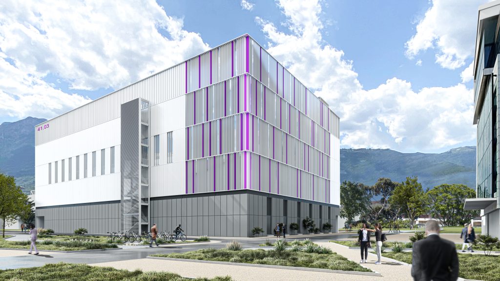
©Unanime Architectes

Serving the European microelectronics industry, the FAMES pilot line aims to advance and strengthen the European Union's semiconductor capabilities and to secure its technological sovereignty.
To foster the development of more efficient, energy-saving, and sustainable chips, FAMES represents an €830 million investment, including 2,000 m² of cleanrooms and nearly 100 new machines.
At the head of FAMES, the CEA is a key player in semiconductor research, recognised for its ability to bring technologies to maturity before transferring them to industry.

Portrait-Julie-Galland

The French government and the European Commission, as part of France 2030 and the Chips Act, have entrusted us with the mission of bringing stakeholders together around our "Lab-to-Fab" model — preparing and transferring semiconductor technologies while anticipating the needs of industry for their future products. To achieve this, we will work closely with all stakeholders — researchers, industrial players, start-ups as well as large corporations — to build true value chains at the European level, driven by R&D and associated training efforts.

Julie Galland

Director of the Technological Research Division - CEA

Portrait-Sebastien-Dauve

FAMES develops semiconductor technologies for markets such as industry, telecommunications, automotive, defense, and healthcare. More than 40 industry stakeholders have already expressed their support and interest in this initiative. Furthermore, the pilot line aims to facilitate and accelerate access to these technologies with performance and energy efficiency as key objectives. Several manufacturers have already begun working with us. We hope to see many of you there to understand and discover what the pilot line can bring to you.

Sébastien Dauvé

CEO - CEA-LETI

Within the Chips Act and France 2030, the European Commission and the French government have entrusted us with the mission of federating stakeholders around our Lab-to-Fab model, preparing and transferring semiconductor technologies while anticipating the needs of industrial partners for their future products. To achieve this, we will work with all actors — academics and manufacturers, from start-ups to major groups — to build real value chains at the European level through R&D and the associated training efforts.

Julie Galland

Director of the Technological Research Division - CEA

Event programme

Event programme

Practical information

Getting to MINATEC

Is this your first visit to the CEA?
Meet us at the MINATEC reception, 3 Parvis Louis Néel - Grenoble.

MINATEC is located near Grenoble train station, which is easily accessible by public transport.

View access map here

Cancelling registration

You've booked a place and you won't be available in the end? Think about cancelling your booking to facilitate organisation and avoid wastage.

To cancel your booking, please contact us at drt@cea.fr

Location

MINATEC

3 parvis Louis Néel

Grenoble

Event contact

drt@cea.fr

Find out more about the FAMES Pilot Line

Visit the Fames website: https://fames-pilot-line.eu/